The development of any electronic device is accompanied by physical or mathematical modeling. Physical modeling is associated with high material costs, since it requires the manufacture of models and their laborious research. Physical modeling is often not possible due to the extreme complexity of the device, for example, in the design of large and very large integrated circuits. In this case, they resort to mathematical modeling using the means and methods of computer technology.
For example, the well-known P-CAD package contains a block of logical modeling of digital devices, but for beginners, including students, it presents significant difficulties in mastering. No less difficulties are encountered when using the DesignLab system. As the analysis of the state of the circuitry modeling software has shown, at the stage of the initial development of computer-aided design methods and at the stages of conducting prospecting and research work, it is advisable to consider the possibility of using the following programs such as Electronics Workbench - EWB.
The circuit simulation system Electronics Workbench is designed to simulate and analyze electrical circuits in Fig. 1. It is correct to say: the Electronics Workbench system for modeling and analyzing electrical circuits, but for brevity, hereinafter, we will call it a program.
The Electronics Workbench program allows simulating analog, digital and digital-to-analog circuits of a high degree of complexity. The libraries available in the program include a large set of widely used electronic components. It is possible to connect and create new component libraries.

Component parameters can be changed in a wide range of values. Simple components are described by a set of parameters, the values of which can be changed directly from the keyboard, active elements - by a model, which is a set of parameters and describes a specific element or its ideal representation.
The model is selected from the list of component libraries, the model parameters can also be changed by the user. A wide range of devices allows you to measure various quantities, set input influences, build graphs. All devices are depicted as close to real as possible, so working with them is simple and convenient.
The simulation results can be output to a printer or imported into a text or graphic editor for further processing. Electronics Workbench software is compatible with P-SPICE software, that is, it provides the ability to export and import diagrams and measurement results in its various versions.
The main advantages of the program
Saving time Working in a real laboratory requires a lot of time to prepare an experiment. Now, with the advent of the Electronics Workbench, the electronic lab is always at hand, making the study of electrical circuits more accessible. Measurement reliability
In nature, there are no two completely identical elements, that is, all real elements have a wide range of values, which leads to errors in the course of the experiment. In Electronics Workbench, all elements are described by strictly set parameters, therefore, each time during the experiment, the result will be repeated, determined only by the parameters of the elements and the calculation algorithm.
Convenient Measurements Learning is impossible without errors, and errors in a real laboratory are sometimes very expensive for the experimenter. Working with the Electronics Workbench, the experimenter is insured against accidental electric shock, and the devices will not fail due to an incorrectly assembled circuit. Thanks to this program, the user has at his disposal such a wide range of devices that will hardly be available in real life.
Thus, you always have a unique opportunity to plan and conduct a wide range of studies of electronic circuits with a minimum amount of time. Graphic capabilities Complex circuits take up a lot of space, while trying to make the image denser, which often leads to errors in connecting conductors to circuit elements. Electronics Workbench allows you to place the circuit in such a way that all the connections of the elements and at the same time the entire circuit are clearly visible.
The intuitiveness and simplicity of the interface makes the program accessible to anyone familiar with the basics of using Windows. P-SPICE Compatibility The Electronics Workbench software is based on standard SPICE software elements. This allows you to export various models of elements and carry out processing of the results using the additional capabilities of different versions of the P-SPICE program.
Components and Experiments
The program component libraries include passive elements, transistors, controlled sources, controlled switches, hybrid elements, indicators, logic elements, trigger devices, digital and analog elements, special combinational and sequential circuits.
Active elements can be represented by models of both ideal and real elements. It is also possible to create your own models of elements and add them to the libraries of elements. The program uses a large set of instruments for measurements: ammeter, voltmeter, oscilloscope, multimeter, Bode plotter (plotter of frequency characteristics of circuits), function generator, word generator, logic analyzer and logic converter.
Circuit Analysis Electronics Workbench can analyze AC and DC circuits. DC analysis determines the steady state operating point of the circuit. The results of this analysis are not reflected in the instruments, they are used for further circuit analysis. AC analysis uses the results of DC analysis to generate linearized models of nonlinear components.
Analysis of circuits in the AC mode can be carried out in both the time and frequency domains. The program also allows you to analyze digital-to-analog and digital circuits. In Electronics Workbench, you can investigate the transients when the circuit is influenced by input signals of various shapes.
Analysis operations:
Electronics Workbench allows you to build circuits of varying degrees of complexity using the following operations:
... selection of elements and devices from libraries,
... moving elements and diagrams to any place of the working field,
... rotation of elements and groups of elements by angles that are multiples of 90 degrees,
... copying, pasting or deleting elements, groups of elements, fragments of schemes and whole schemes,
... color change of conductors,
... color highlighting of the contours of the schemes for a more convenient perception,
... simultaneous connection of several measuring devices and observation of their readings on the monitor screen,
... assigning a symbol to an element,
... changing the parameters of elements in a wide range. All operations are performed using the mouse and keyboard. Control only from the keyboard is not possible.
By configuring the devices, you can:
... change the instrument scales depending on the measurement range,
... set the operating mode of the device,
... set the type of input influences on the circuit (direct and harmonic currents and voltages, triangular and rectangular pulses).
The graphic capabilities of the program allow:
... simultaneously observe several curves on the graph,
... display curves on graphs in different colors,
... measure the coordinates of points on the graph,
... import data into a graphics editor, which allows you to make the necessary transformations of the picture and output it to the printer.
Electronics Workbench allows using the results obtained in P-SPICE, PCB programs, as well as transferring results from Electronics Workbench to these programs. You can insert a diagram or its fragment into a text editor and print explanations or notes on the operation of the diagram in it.
Working with Electronics Workbench
Electronics Workbench software is designed to simulate and analyze electronic circuits. The capabilities of the Electronics Workbench v.5 program are approximately equivalent to the capabilities of the MicroCap program and allow you to perform work from the simplest experiments to statistical modeling experiments.
When creating a schematic, the Electronics Workbench allows you to:
-select elements and devices from libraries,
Move elements and diagrams to any place in the working area,
Rotate elements and their groups by angles in multiples of 90 degrees,
Copy, paste or delete elements, fragments of circuits,
Change the colors of the conductors,
Highlight the outline of the schemes,
Simultaneously connect several measuring devices and observe their readings on the monitor screen,
- assign symbols to elements,
Change parameters of elements.
By changing the device settings, you can:
- change the instrument scales depending on the measurement range,
Set the operating mode of the device,
Set the type of input influences on the circuit (direct or harmonic currents or voltages, triangular or rectangular pulses).
Insert a diagram or its fragment into a text editor, in which an explanation of the diagram's operation is printed.
Electronics Workbench components
After launching WEWB32, the menu bar and component bar appear on the screen.
The component panel consists of icons of the component fields, and the component field - of the symbolic representations of the components.
Clicking on the component icon opens the field corresponding to this icon.
Following are some of the elements from the component fields:
Basic (basic components)

Connecting knot
The node is used to connect conductors and create control points.
Resistor
Resistor resistance can be specified as a number in Ohm, kOhm, MOhm
Capacitor
the capacitance of the capacitor is set by a number indicating the dimension (pF, nF, μF, mF, F).
Key
Key operated by key. Such keys can be closed or opened using controlled keys on the keyboard. (The name of the control key can be entered from the keyboard in the dialog box that appears after double-clicking on the key image.)
Sources

Land
The "Ground" component has zero voltage and serves as a reference point for the potentials.
DC voltage source 12V
EMF of a constant voltage source is indicated by a number indicating the dimension (from μV to kV)
DC power supply 1A
DC source current is specified by a number with dimension indication (from μA to kA)
AC voltage source 220 V / 50 Hz

The rms value (root-mean-sguare-RMS) of the source voltage is given by a number with an indication of the dimension (from μV to kV). It is possible to set the frequency and start phase.
AC source 1 A / 1 Hz

The effective value of the source current is specified by a number with the indicated dimension (from μA to kA). It is possible to set the frequency and start phase.
Clock generator 1000 Hz / 50%

The generator generates a periodic sequence of rectangular pulses. Pulse amplitude, duty cycle and pulse repetition rate can be adjusted.
Indicators

The simplest instruments are a voltmeter and an ammeter. They automatically change the measuring range. Several such devices can be used simultaneously in one circuit.
Voltmeter

A voltmeter is used to measure AC or DC voltage. The bold side of the rectangle corresponds to the negative terminal.
Double-clicking on the voltmeter image opens a dialog box for changing the voltmeter parameters:
-values of internal resistance (default 1MΩ),
- the type of measured voltage (DC-constant, AC-variable).
When measuring alternating sinusoidal voltage (AC), the voltmeter shows the rms value
Ammeter
![]()
An ammeter is used to measure AC or DC current. The bold side of the rectangle corresponds to the negative terminal.
Double-clicking on the ammeter image opens a dialog box for changing the ammeter parameters
Internal resistance values (default 1mOhm),
Type of measured voltage (DC-constant, AC-variable).
When measuring alternating sinusoidal voltage (AC), the ammeter shows the rms value
Instruments

1 .Functional generator
The generator is an ideal voltage source producing sinusoidal, triangular or rectangular waveforms. The middle terminal of the generator, when connected to the circuit, provides a common reference point for the amplitude of the AC voltage. To read the voltage relative to zero, this terminal is grounded. The extreme left and right pins are used to feed a signal to the circuit. The voltage on the right terminal changes in the positive direction relative to the common terminal, on the left terminal in the negative direction.
When you double-click on the generator image, an enlarged image of the generator opens, where you can set:
- the form of the output signal,
- the frequency of the output voltage (Frequency),
- Duty cycle,
- the amplitude of the output voltage (Amplitude),
- constant component of the output voltage (Offset).

2. Oscilloscope
The oscilloscope image has four input terminals
- upper right clamp - common,
- lower right - synchronization input,
- the bottom left and right terminals represent the Channel A and Channel B inputs, respectively.
Double-clicking on the oscilloscope's thumbnail image opens an image of a simple oscilloscope model on which you can install
- the position of the axes along which the signal is deposited,
- the required scale of the scan along the axes,
- offset of the origin along the axes,
- capacitive input (AC button) or potential input (DC button) channel,
- synchronization mode (internal or external).

The Trigger field is used to determine when the sweep starts on the oscilloscope screen. The buttons in the Edge row set the moment when the oscillogram is triggered by the rising or falling edge of the pulse at the synchronization input. The Level field allows you to set the level above which the sweep starts.
Auto, А, В, Ext buttons set the synchronization modes
-Auto - automatic start of the sweep when the circuit is turned on. When the beam reaches the end of the screen, the waveform is recorded from the beginning of the screen,
-A - the triggering signal is the signal arriving at the input A,
-B - the triggering signal is the signal arriving at the input B,
-Ext - External launch. In this case, the trigger signal is the signal applied to the sync input.
Pressing the EXPAND button on a simple scope model opens the expanded scope model. In contrast to the simple model, there are three information boards on which the measurement results are displayed. In addition, a scroll bar is located directly under the screen, allowing you to observe any time period from the moment of switching on to the moment of switching off the circuit.

The oscilloscope screen contains two cursors (red and blue), designated 1 and 2, with which you can measure instantaneous voltage values at any point in the oscillogram. To do this, the cursors are dragged with the mouse to the required position (with the mouse, they grab the triangles at the top of the cursor).
The coordinates of the points of intersection of the first cursor with the waveforms are displayed on the left panel, the coordinates of the second cursor on the middle panel. The right panel displays the values of the differences between the corresponding coordinates of the first and second cursors.
The Reduce button takes you to a simple oscilloscope model.
3. Plotter (Bode plotter)
Used to build amplitude-frequency (AFC) and phase-frequency<ФЧХ) характеристик схемы.
The plotter measures the ratio of signal amplitudes at two points in the circuit and the phase shift between them. For measurements, the plotter generates its own frequency spectrum, the range of which can be set during instrument setup. The frequency of any alternating source in the circuit under study is ignored, but the circuit must include some kind of AC source.
The plotter has four terminals: two input (IN) and two output (OUT). The left pins of the IN and OUT inputs are connected to the test points, and the right pins of the IN and OUT inputs are grounded.
When you double-click on the plotter image, its enlarged image opens.

The MAGNITUDE button is pressed to obtain the frequency response, the PHASE button - to obtain the phase response.
The VERTICAL panel sets:
-initial (I) value of the parameter of the vertical axis,
-final (F) value of the parameter of the vertical axis
- type of vertical axis scale - logarithmic (LOG) or linear (LIN).
The HORIZONTAL panel is configured in the same way.
When receiving the frequency response along the vertical axis, the voltage ratio is plotted:
-in a linear scale from 0 to 10E9;
-in a logarithmic scale from - 200 dB to 200 dB.
When the phase-frequency characteristic is obtained, the degrees from -720 degrees to +720 degrees are plotted along the vertical axis.
The horizontal axis is always the frequency in Hz or in derived units.
The cursor is located at the beginning of the horizontal scale. The coordinates of the point of movement of the cursor with the graph are displayed on the information fields at the bottom right.

Modeling circuits
The investigated circuit is assembled on the working field using a mouse and keyboard.
When building and editing circuits, the following operations are performed:
-selection of a component from a library of components;
-allocation of an object;
-movement of the object;
-copying objects;
-deleting objects;
-connection of circuit components with conductors;
-setting the values of the components;
-connection of measuring devices.
After building the circuit and connecting the devices, the analysis of the circuit operation begins after pressing the switch in the upper right corner of the program window (while the circuit time moments are shown in the lower left corner of the screen).
Pressing the switch again will terminate the circuit.
You can pause the circuit by pressing the F9 key on the keyboard; pressing F9 again restarts the circuit (a similar result can be achieved by pressing the Pause button located under the switch.)
The choice of the component necessary for the construction of the circuit is made after the selection of the component field containing the required element. This element is grabbed by the mouse and moved to the working area.
Selection of an object. When selecting a component, left-click on it. This makes the component red. (You can remove the selection by clicking anywhere in the working area.)
Moving an object. To move an object, select it, set the mouse pointer over the object and, holding down the left mouse button, drag the object.
The object can be rotated. To do this, the object must first be selected, then right-click and select the required operation
-Rotate (rotate 90 degrees),
-Flip vertical (vertical flip),
-Flip horizontal
Copying objects is carried out by the command Soru from the Edit menu. The object must be selected before copying. When the command is executed, the selected object is copied to the clipboard. To paste the contents of the buffer into the working field, select the Paste command from the Edit menu
Removing objects. Selected objects can be deleted with the Delete command.
Connecting circuit components with conductors. To connect the components with wires, you need to move the mouse pointer over the component pin (a black dot will appear on the pin). While holding down the left mouse button, move the mouse pointer to the component pin you want to connect to, and release the mouse button. The component leads are connected with a conductor.
The color of the conductor can be changed by double-clicking on the conductor with the mouse and choosing the desired color from the window that appears.
Removing a conductor. If for any reason a conductor needs to be deleted, you must move the mouse pointer to the component output (a black dot should appear). Pressing the left mouse button, move it to an empty place in the working area and release the mouse button. The explorer will disappear.
Parameter values are set in the component properties dialog box, which is opened by double-clicking on the component's image (Value tab).
Each component can be named (Label Tab)
Connecting devices. To connect the device to the circuit, you need to drag the device from the toolbar to the working field with the mouse and connect the device leads to the points under study. Some instruments must be grounded or their readings will be incorrect.
An enlarged image of the device appears when you double-click on the thumbnail image.
Exercise: Assemble the voltage divider circuit shown in the figure.
- Apply a sinusoidal voltage with a frequency of 3 kHz and an amplitude of 5 V to the input of the circuit from the function generator,
-Connect the same signal to channel A of the oscilloscope,
-Connect channel B of the oscilloscope to the divider output,
- highlight the conductors of channel A and channel B with different colors,
-Turn on the circuit, if necessary change the settings of the measuring instruments,
-Go to the advanced oscilloscope model. Using the cursor and the left bulletin board, measure the amplitude value of the output signal.
- Additionally connect voltmeters to the input and output and turn on the circuit again.
Get correct voltmeter readings.

Word generator
A reduced image of the word generator is displayed on the diagram
![]()
Bits of the generated word are fed in parallel to 16 outputs at the bottom of the generator.
The clock output (bottom right) is supplied with a sequence of clock pulses with a specified frequency.
The sync input is used to provide a sync pulse from an external source.
Double click to open the extended generator image

The left side of the generator contains 16-bit words, specified in hexadecimal code. Each code combination is entered using the keyboard. The number of the edited cell (from 0 to 03FF, i.e. from 0 to 2047) is highlighted in the Edit window. In the process of generator operation in the Address compartment, the address of the current cell (Current), the starting cell (Initial) and the ending cell (Final) is indicated. Code combinations issued to 16 outputs (at the bottom of the generator) are indicated in ASCII code and binary code (Binary).
The generator can operate in stepping, cyclic and continuous modes.
-The Step button switches the generator to step-by-step mode;
- Burst button - in cyclic mode (all words are sent to the generator output once sequentially;
-Button Cycle - in continuous mode. To interrupt continuous operation, press the Cycle button again.
The Trigger panel determines the moment of the generator start (Internal - internal synchronization, External - external synchronization when data is ready.)
External synchronization mode is used when the DUT can acknowledge (acknowledge) the receipt of data. In this case, a signal from the Data ready terminal is sent to the device along with the code combination, and the DUT must issue a data acquisition signal, which must be connected to the Trigger terminal of the word generator. This signal also makes the next start of the generator.
The Breakpoint button interrupts the generator in the specified cell. To do this, select the required cell with the cursor, and then press the Breakpoint button
The Pattern button opens a menu with which you can
Clear buffer - erase the contents of all cells,
Open - load code combinations from a file with the .dp extension.
Save - save all combinations typed on the screen to a file;
Up counter - fill the screen buffer with code combinations, starting from 0 in the zero cell and then adding one in each subsequent cell;
Down counter - fill the screen buffer with code combinations, starting with FFFF in the zero cell and then decreasing by 1 in each subsequent cell;
Shift right - fill every four cells with combinations of 8000-4000-2000-1000 with their shift in the next four cells to the right;
Shift left is the same, but shifted to the left.
Logic analyzer
A reduced image of the logic analyzer is displayed on the circuit
The logic analyzer is connected to the circuit using the pins on the left side. Signals can be observed simultaneously at 16 points of the circuit. The analyzer is equipped with two cross-hairs, which allows to obtain readings of time intervals T1, T2, T2-T1, as well as a horizontal scroll bar

The Clock block has terminals for connecting a conventional External and Selective Qualifier trigger sources, the parameters of which can be set using the menu invoked by the Set button.
Triggering can be done on the rising edge (Positive) or the falling (Negative) edge of the trigger signal using an External or Internal source. In the Clock qualifier window, you can set the value of the logical signal (0.1 or x) at which the analyzer starts.
External synchronization can be performed by a combination of logic levels applied to the analyzer channel inputs.
ELECTRONICS WORKBENCH PROGRAM
Electronics Workbench Features
The Electronics Workbench program allows simulating analog, digital and digital-to-analog circuits of a high degree of complexity. The libraries available in the program include a large set of models of widely used electronic elements (components). Simple elements are described by a set of parameters, the values of which can be changed directly from the keyboard, active elements - by a model, which is a set of parameters and describes a specific element or its ideal representation. The model is selected from the list of element libraries, the model parameters can also be changed by the user.
The program element libraries include models of passive elements, transistors, controlled sources, controlled keys, hybrid elements, indicators, logic elements, trigger devices, digital and analog elements, special combinational and sequential circuits. It is also possible to create your own models of elements and add them to libraries.
The program uses a large set of instruments for measurements: ammeter, voltmeter, oscilloscope, multimeter, bode-plotter (plotter of frequency characteristics of circuits), function generator, word generator, logic analyzer and logic converter.
The Electronics Workbench allows you to analyze AC and DC circuits. DC analysis determines the parameters of the circuit in a steady state. AC analysis can be performed in both the time and frequency domains. You can investigate the transients when the circuits are exposed to input signals of various shapes.
Analysis operations:
Selection of elements and devices from libraries,
Moving elements and diagrams to any place in the working field,
Rotation of elements and groups of elements by angles that are multiples of 90 degrees,
Copying, pasting or deleting elements, groups of elements, fragments of schemes and entire schemes,
Change the color of the conductors,
Highlighting the outlines of circuits in color for a more convenient perception,
Simultaneous connection of several measuring devices and observation of their readings on the monitor screen,
Assigning a symbol to an element,
Changing the parameters of elements in a wide range.
All operations are performed using the mouse and keyboard. Control only from the keyboard is not possible. By configuring the devices, you can:
Change the instrument scales depending on the measurement range,
Set the operating mode of the device,
Set the type of input influences on the circuit (direct and harmonic currents and voltages, triangular and rectangular pulses).
The graphic capabilities of the program allow:
Simultaneously observe several curves on the graph,
Display curves on graphs in different colors,
Measure the coordinates of points on the graph,
Import data into a graphics editor, which allows you to make the necessary transformations of the picture and output it to the printer.
Electronics Workbench allows you to insert a diagram or a fragment of it into a text editor and print explanations or notes on the operation of the diagram in it.
Electronics Workbench Elements
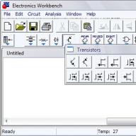
For operations with elements of electrical and electronic circuits on the general field of Electronics Workbench, two areas are highlighted: the panel of elements and the field of elements (Fig. & 1.1). The toolbox consists of field icons, and the toolbox consists of their conventional images. By clicking on one of the thirteen icons located on the panel, you can open the corresponding field.
In fig. 1.1 the Sources field is open. The arrangement of elements in the fields is focused on the frequency of their use. To describe the elements, it is more logical to divide them by types. All elements used in the Electronics Workbench program can be conditionally divided into the following groups: sources, basic elements, linear elements, keys, nonlinear elements, indicators, logic elements, combination type nodes, sequential type nodes, hybrid components. In fig. 1. 2 shows all the element fields available in the Electronics Workbench. This picture is obtained artificially, in fact, only one field of elements can be opened during operation.

Sources of
All sources in the Electronics Workbench are perfect. The internal resistance of an ideal voltage source is zero, so its output voltage is independent of the load. If it is necessary to use two voltage sources connected in parallel, a small resistance should be connected in series between them (for example, 1 Ohm). An ideal current source has an infinite internal resistance, so its current is independent of the load resistance.
The EMF of a constant voltage source is measured in Volts and is given by derived quantities (from μV to kV). A short bold line in the battery image denotes a terminal that has a negative potential with respect to the other terminal.
The direct current is measured in amperes and given in derived quantities (μA to kA). The arrow indicates the direction of the current (from "+" to "-").
The rms value (root-mean-square - RMS) of the source voltage is measured in Volts and given by derived values (from μV to kV). It is possible to set the frequency and start phase. The effective value of the voltage V RMS generated by the source is related to its amplitude value V PEAK by the following relationship:

The effective value of the source current is measured in Amperes and is given by derived values (from μA to kA). It is possible to set the frequency and start phase. The effective value of the current I RMS is related to its amplitude value I PEAK as follows:

The generator generates a sequence of rectangular pulses. You can adjust the pulse amplitude, duty cycle (duty cycle) and pulse repetition rate. The amplitude of the generator pulses is counted from the terminal opposite to the "+" terminal.
The output voltage of a voltage controlled voltage source depends on the input voltage applied to the control terminals. The ratio of the output voltage to the input voltage is determined by the proportionality coefficient E, which is set in mV / V, V / V and kV / V:
where Vout is the output voltage of the source, Vin is the input voltage of the source.
The amount of current of the voltage controlled current source depends on the input voltage applied to the control terminals. The ratio of the output current to the control voltage is the G factor, measured in units of conductivity (1 / Ohm or siemens):
where I out is the output current of the source, V in is the voltage applied to the control terminals of the source.
The input and output currents of this source are related by the proportional factor F. The F factor is specified in mA / A, A / A and kA / A.
where I out is the output current of the source, I in is the input current of the source.
The magnitude of the voltage of the source controlled by the current depends on the magnitude of the input current (current in the control branch). The input current and the output voltage form a parameter called the transfer resistance H, which is the ratio of the output voltage to the control current. Transfer resistance has the dimension of resistance and is set in Ohm, kOhm and mOhm
where V ou t is the output voltage of the source, I in is the input current of the source.
When connecting controlled sources, the polarity and direction of currents in the connected circuits must be observed. The arrow indicates the direction of the current from "+" to "-".
Using this voltage source, it is possible to set the node to a fixed potential of 5 V or to a logic-high level.
With the help of this source, the level of a logical unit in the circuit node is set.
Basic elements
The node is used to connect wires and create control points. A maximum of four conductors can be connected to each node. After the circuit is assembled, you can insert additional nodes for connecting devices.
The ground component is at zero voltage and thus provides a reference point for the potentials. Not all circuits need to be grounded for simulation, however, any circuit containing: an operational amplifier, a transformer, a controlled source, an oscilloscope must be grounded, otherwise the instruments will not make measurements or their readings will turn out to be incorrect.
Linear elements
The resistance of the resistor is measured in ohms and is given in derived quantities (from ohms to megohms).
The position of the variable resistor slider is set using a special element - a regulator arrow. In the dialog box, you can set the resistance, the starting position of the slider (in percent) and the increment (also in percent). It is possible to change the position of the slider using the keys-keys.
Keys used:
Letters from A to Z,
Digits from 0 to 9,
Enter key on your keyboard,
Spacebar.
To change the position of the slider, you must press the key. To move the slider upwards, it is necessary to simultaneously press the key-key, to the smaller side, only the key-key.
Example: The slider is set to 45%, the increment is 5%, the key is the space bar. By pressing the keys, we move the slider to the 40% position. Each time the key is pressed, the value decreases by 5%. If you press +, then the position of the potentiometer slider will increase by 5%.
The capacitance of a capacitor is measured in Farads and is given by derived quantities (from pF to F).
The variable capacitor allows for the possibility of changing the value of the capacitance. The capacity is set using its initial value and the value of the proportionality coefficient as follows: C = (initial value / 100) proportionality coefficient. The capacitance value can be set using the keys-keys in the same way as the position of the variable resistor slider.
The inductance of the coil (choke) is measured in Henry and is given by derived values (from μH to H).
The value of the inductance of this coil is set using its initial value and the value of the proportional factor as follows: L = (initial value / 100) factor. The inductance value can be set using the keys-keys in the same way as the position of the variable resistor slider.
A transformer is used to convert voltage VI to voltage V2. Transformation ratio n is equal to the ratio of the voltage VI on the primary winding to the voltage V2 on the secondary winding. Parameter n can be set in the properties dialog of the transformer model. The transformer can be designed with a midpoint tap.
The circuit containing the transformer must be grounded.
Keys
Keys have two states: off (open) and on (closed). In the off state, they represent an infinitely large resistance, in the on state, their resistance is zero. Keys can be controlled:
With the key,
Timer,
Voltage,
Since the closed keys in Electronics Workbench have a resistance equal to zero, then when connected in parallel with another key or with a voltage source, it is recommended to introduce a 1 Ohm resistor in series into the circuit.
An electromagnetic relay can have normally closed or normally open contacts. It picks up when the current in the control winding exceeds the pickup current I on. During operation, a pair of normally closed contacts S2, S3 of the relay switches to a pair of normally open contacts S2, S1. The relay remains in the activated state as long as the current in the control winding exceeds the holding current I hd. The current I hd must be less than I on.
Keys can be closed or opened using the control keys on the keyboard. The name of the control key can be entered from the keyboard in the dialog box that appears after double-clicking on the key image.
Example: If you want to change the state of the key with the "space" key, you should enter the word "Space" in the dialog box and click OK.
Keys used: letters from A to Z, numbers from 0 to 9, the Enter key on the keyboard, the space key.
The time relay is a key that opens at time T off and closes at time T on. T on and T off must be greater than 0. If T on< T off , то в начальный момент времени, когда t = 0, ключ находится в разомкнутом состоянии. Замыкание ключа происходит в момент времени t = T on , а размыкание - в момент времени t = T off . Если T on >T off, then at the initial moment of time, when t = 0, the key is in a closed state. The key is opened at the time t = T off, and the key is closed at the time t = T on. T on cannot equal T off.
The voltage-controlled switch has two control parameters: turn-on (V on) and turn-off (V off) voltages. It closes when the control voltage is greater than or equal to the turn-on voltage V on and opens when it is equal to or less than the turn-off voltage V off.
The current-controlled switch works in the same way as the voltage-controlled switch. When the current through the control terminals exceeds the turn-on current I on, the switch is closed; when the current falls below the shutdown current I off - the key is opened.
Non-linear elements
An incandescent lamp is a resistive type element that converts electricity into light energy. It is characterized by two parameters: maximum power P max and maximum voltage V max. The maximum power can be in the range from mW to kW, the maximum voltage in the range from mV to kV. When the voltage on the lamp is greater than V max (at this moment, the power released in the lamp exceeds P m ax), it burns out. In this case, the image of the lamp changes (the filament breaks) and its conductivity becomes zero.
The fuse breaks the circuit if the current in it exceeds the maximum current I max. The I max value can range from mA to kA. In circuits where AC sources are used, I max is the maximum instantaneous, and not the effective value of the current.
The current through the diode can only flow in one direction - from the anode A to the cathode K. The state of the diode (conducting or non-conducting) is determined by the polarity of the voltage applied to the diode.
For a zener diode (Zener diode), the working voltage is negative. Usually this element is used to stabilize the voltage.
An LED emits visible light when the current passing through it exceeds a threshold.
The bridge rectifier is designed to rectify AC voltage. When a sinusoidal voltage is applied to the rectifier, the average value of the rectified voltage V dc can be approximately calculated by the formula:
where V p is the peak value of the sinusoidal voltage.
The Schottky diode is in the off state until the voltage across it exceeds a fixed threshold voltage level.
The thyristor, in addition to the anode and cathode leads, has an additional control electrode lead. It allows you to control the moment of transition of the device to the conducting state. The valve is opened when the gate current exceeds the threshold value and a positive voltage is applied to the anode terminal. The thyristor remains open until a negative voltage is applied to the anode terminal.
The triac is capable of conducting current in two directions. It is locked when the polarity of the current flowing through it changes and is unlocked when the next control pulse is applied.
Dinistor is an anode voltage controlled bi-directional switch. The dynistor does not conduct current in until the voltage across it. When the voltage applied to the dynistor exceeds the switching voltage, the latter becomes conductive and its resistance becomes zero.
An operational amplifier (OA) is an amplifier designed to work with feedback. It usually has a very high voltage gain, high input impedance and low output impedance. The "+" input is direct and the "-" input is inverting. The operational amplifier model allows you to set the parameters: gain, offset voltage, input currents, input and output resistance. The op amp inputs and outputs must be referenced to ground.
A five-pin op amp has two additional pins (positive and negative) for connecting power. The Boole-Koch-Pederson model is used to simulate this amplifier. It takes into account second order effects, limiting the output voltage and current.
A multiplier multiplies the two input voltages V x and V y. The output voltage V out is calculated using the formula:
![]() .
.
where k is a multiplication constant that can be set by the user.
Bipolar transistors.
Bipolar transistors are current controlled amplifying devices. They are of two types: p-n-p and n-p-n. The letters indicate the type of conductivity of the semiconductor material from which the transistor is made. In both types of transistors, the arrow marks the emitter, the direction of the arrow indicates the direction of current flow.
The n-p-n transistor has two n-type regions (collector k and emitter e) and one p-type region (base b).
Field Effect Transistors (FET)
FETs are controlled by the gate voltage, that is, the current flowing through the transistor depends on the gate voltage. The field effect transistor includes an extended region of an n-type or p-type semiconductor called a channel. The channel is equipped with two electrodes called source and drain. In addition to the n-or p-type channel, the field-effect transistor includes a region with a conduction type opposite to the channel. An electrode connected to this area is called a gate. For field-effect transistors, the Electronics Workbench has a dedicated field of FET components. There are three types of field-effect transistors in the program: pn junction transistors (JFETs) and two types of metal oxide transistors (MOSFETs or MOSFETs): MOSFETs with an embedded channel (Depletion MOSFETs) and MOSFETs with induced channel (Enhancement MOSFETs).
Junction Field Effect Transistors (JFET)
A pn junction field effect transistor (JFET) is a voltage controlled unipolar transistor that uses an induced electric field, dependent on gate voltage, to control current. For an n-channel field-effect transistor with a control pn junction, the current increases with increasing voltage. In the component field, there are two types of such transistors: n-channel and p-channel.
Metal Oxide Field Effect Transistors
The current flowing through a metal oxide field effect transistor (MOSFET or MOSFET) is also controlled by an electric field applied to the gate. Typically, the substrate contacts the most negatively biased source terminal of the transistor. In three-terminal transistors, the substrate is internally connected to the source. The N-channel transistor has the following designation: the arrow is directed towards the inside of the icon; The p-channel transistor has an arrow coming out of the icon. N-channel and p-channel MOS transistors have different polarity of control voltages. There are 8 types of MOSFETs in Electronics Workbench: 4 types of MOSFETs with an embedded channel, 4 types of MOSFETs with an induced channel.
Depletion MOSFETs
Like junction field-effect transistors (JFETs), an embedded channel MOSFET consists of an extended region of semiconductor called a channel. For a p-channel transistor, this region is a p-type semiconductor, for an n-channel transistor, it is an n-type. The metal gate of the MOSFET is insulated from the channel by a thin layer of silicon dioxide so that the gate current is negligible during operation. The drain current of an n-channel transistor is determined by the gate-source voltage. With an increase in this voltage, the current increases, with a decrease in voltage, it decreases. At the gate-source voltage Vgs (off), the channel is completely depleted and the current from the source to the drain stops. The voltage Vgs (off) is called the cut-off voltage. On the other hand, the more positive the gate-source voltage, the larger the channel size, which increases the current. The P-channel transistor works in a similar way, but with opposite voltage polarities.

MOSFETs with induced channel
These MOSFETs do not have a physical channel between source and drain like embedded channel MOSFETs. Instead, the conduction region can expand to cover the entire silicon dioxide layer. The induced channel MOSFET operates only when the source-gate voltage is positive. A positive source-gate voltage above the minimum threshold (Vto) creates an inversion layer in the conduction region adjacent to the silicon dioxide layer. The conductance of this induced channel increases with increasing positive gate-source voltage. MOSFETs with induced channel are used primarily in digital and highly integrated circuits (LSI).

Digital elements
The digital elements of the program are represented by the following groups: indicators, logical elements, combination-type nodes, sequential-type nodes, hybrid elements.
Indicators
Each of the seven indicator pins controls a corresponding segment, a through g. The operation table shows combinations of logic levels that must be set at the input of the indicator in order to get images of hexadecimal digits from 0 to F. on its display.
The designation of the segments of the seven-segment display and the table of functioning are shown below:
Functioning table
| a | b | With | d | e | f | g | display symbol | |
| - | ||||||||
| A | ||||||||
| b | ||||||||
| WITH | ||||||||
| d | ||||||||
| E | ||||||||
| F |
The decoding seven-segment indicator serves to display on its display hexadecimal numbers from 0 to F, set by the state at the indicator input. The correspondence of the states on the terminals to the displayed symbol is given in the table of functioning.
Functioning table
| a | b | With | d | display symbol |
| . 1 | A | |||
| b | ||||
| WITH | ||||
| d | ||||
| E | ||||
| F |
The probe determines the logic level (0 or 1) at a specific point in the circuit. If the investigated point has a logic level of 1, the indicator lights up red. The logical zero level is not marked with a glow. Use the Value command on the Circuit menu to change the glow color of the probe.
The buzzer is used for audible signaling of excess voltage supplied to it. The computer's built-in speaker emits a sound at a specified frequency if the voltage exceeds the threshold. Use the Value command on the Circuit menu to set the threshold voltage and frequency for the beep.
Logic gates
Electronics Workbench contains a full set of logic elements and allows you to set their basic characteristics, including the type of element: TTL or CMOS. The number of inputs of logic elements of the circuits can be set in the range from 2 to 8, but there can be only one output of the element.
A logical NOT element or an inverter changes the state of the input signal to the opposite. The logic level 1 appears at its output, when the input is 0.
Truth table
Boolean Algebra Expressions:
The AND-NOT element implements the function of logical multiplication with the subsequent inversion of the result. It is represented by a model of consecutively included AND and NOT elements. The truth table of the item is obtained from the truth table of the item AND by inverting the result.
Truth table
The buffer type can be set using the Model command on the Circuit menu (CTRL + M). When using a TTL element as a buffer, you must select the LS-BUF or LS-OC-BUF (Open Collector) buffer model. If a CMOS element is used as a buffer, the HC-BUF or HC-OD-BUF (Open Drain) model should be selected. If no buffer type is selected, the buffer behaves like a normal low-load digital element.
The tri-state buffer has an additional enable input. If there is a high potential at the enabling input, then the element operates according to the truth table of an ordinary buffer, if it is low, then regardless of the signal at the input, the output will go into a state with high impedance. In this state, the buffer does not pass the input signals.
Setting the operating mode is done in the same way as for a normal buffer.
The Electronics Workbench package is designed for modeling and analyzing electrical and circuitry diagrams. This package with a high degree of accuracy simulates the construction of real circuits in hardware.
Table 3
Pictogram menu
|
Pictogram |
Name |
Description |
|
Favorites |
||
|
Signal sources |
||
|
Passive components and switching devices |
||
|
Transistors |
||
|
Analog microcircuits |
||
|
Mixed microcircuits |
||
|
Digital microcircuits |
||
|
Logic digital microcircuits |
||
|
Digital microcircuits |
||
|
Indicator devices |
||
|
Analog Computing Devices |
||
|
Mixed components |
||
|
Instrumentation |
Basic techniques of work
In Electronics Workbench, circuit assembly is done in the workspace. Electronic components for assembling the circuit are taken from the menu containing a set of components. The contents of a set of components can be changed by clicking the corresponding buttons located directly above the windows. To move the required component to the work area, place the cursor on it and press the left mouse button. Then, while holding down the key, "drag" the element by moving the mouse to the desired position in the work area and release the key.
To perform any operations on an element, it must be selected. An element is selected by clicking on the element, and it turns red.
If you need to rotate an element, you must first select it, and then use a combination of keys, pressing which rotates the element by 90 °.
To delete an element, you must also first select it, and then press the key and, in response to the request for confirmation of deletion, press the button to confirm or cancel deletion.
All electronic components are characterized by their own parameters that determine their behavior in the circuit. To set these parameters, you need to double-click on the desired element, as a result of which a dialog box will appear in which you must select or write the required parameters and close it by clicking the button Ok .
To connect the leads of the elements, move the cursor to the desired output, and if it is really possible to connect a conductor to this output, a small black circle will appear on it. When a circle appears, press the left mouse button and, without releasing it, drag the cursor to another pin. When a black circle appears on the other pin too, release the key and these pins will automatically be connected with a conductor. If the element pin is to be connected to an existing conductor, then move the mouse cursor to this conductor while pressing the key, and a small circle will appear in the place where the connection can be made. At this point, release the key, and the circuit will automatically form a conductive connection between the conductors, indicated by a black circle.
Main components
1. Constant voltage source
Found in the set Signal sources
 .
.
This element is a model of an ideal voltage source that maintains a constant voltage of a given value at its terminals. The voltage value can be set by the developer by double-clicking on the element and writing the required value in the dialog box.
Incandescent light bulb
2. Incandescent light bulb.
Found in the set Indicator devices.

This element simulates a conventional incandescent lamp and can be in three states: off, on, and burned out. The behavior of an element is characterized by two parameters: power and maximum allowable voltage. You can enter the required parameters by double-clicking on the element. Then a dialog box appears. Enter the required parameters and close the dialog box by clicking the button Ok .
When the circuit is working, the element will be in off condition if the voltage applied to it does not exceed half the maximum voltage. If the applied voltage is in the range from half the maximum voltage to the maximum voltage level, the cell is in included condition. When the applied voltage exceeds the specified maximum voltage, the element goes into burnt out condition.
Earthing
3. Grounding.
Found in the set Signal sources.
In a circuit assembled using the Electronics Workbench, as in almost any real circuit, it is required to indicate a point of zero potential, relative to which voltages are determined at all other points of the circuit. It is for this purpose that the grounding element serves. Its only output is connected to that point of the circuit, the potential of which is taken to be zero. It is permissible and even advisable, especially for complex circuits, to use several grounding elements. In this case, it is considered that all points to which the grounding is connected have one common potential equal to zero.
Point - connector
4. Point - connector.
Found in the set .

The main property of a connector point is that you can connect conductors to it. You can connect conductors to a point from the left, right, top and bottom, that is, there are only four places for connecting conductors to one point and, therefore, no more than four conductors can be connected at one point. To implement such a connection, you need to bring the conductor with the mouse button pressed to the corresponding side of the point, and a small black circle appears near the point. Releasing at this moment the left mouse button, we get the required connection.
Switch
5. Switch.
Found in the set Passive components and switching devices.
This switch allows two possible positions, in which one common input is connected to one of two possible outputs. By default, switching is done with the spacebar. To assign a different key to a switch, you need to double-click on this switch, enter the required character in the dialog box that appears, and click Ok confirm your choice. After that, the switching of this switch will be carried out using the selected key.
Speaker
6. Speaker.
Found in the set Indicator devices.
This element emits a beep of the specified frequency if the voltage applied to its terminals exceeds the specified voltage level. The values of the threshold voltage and the frequency of the emitted signal can be set in the dialog box that appears when you double-click on the element.
Voltmeter
7. Voltmeter.
Found in the set Indicator devices.
This element shows the voltage applied to its terminals. One of the sides of this element is highlighted with a thickened line. If the voltage applied to the terminals is such that the potential at the terminal located on the non-selected side is greater than the potential at the terminal located on the selected side, then the sign of the voltage indicated by the voltmeter will be positive. Otherwise, the sign of the indicated voltage will be negative.
Ammeter
8. Ammeter.
Found in the set Indicator devices.
This element shows the amount of current flowing through its terminals. One of the sides of this element is highlighted with a thickened line. If the direction of the current flowing through the terminals of the element coincides with the direction from the unselected side to the selected side, then the sign of the magnitude of the indicated current will be positive. Otherwise, the sign will be negative.
Resistor
9. Resistor.
Found in the set. Passive components and switching devices.
This element is one of the most widely used electronic circuit components. The value of the resistance of the resistor is set by the developer in the dialog box that appears when you double-click on the element.
The simplest electrical circuits
The simplest electrical circuit consists of a source and a receiver of electrical energy. The simplest source of electrical energy can be a constant voltage source, such as a battery. The receiver of electrical energy is usually a device that converts the energy of an electric current into another type of energy, for example, into light energy in a light bulb, or into the energy of acoustic waves in dynamics.
To ensure the flow of current through the receiver, it is necessary to form a closed loop through which the current flows. To do this, it is necessary to connect one terminal of the receiver of electrical energy to the negative terminal of the battery, and the other to the positive terminal. The simplest way to control the flow of current through a circuit is to open and close the circuit with a switch. Opening the circuit will open the circuit, causing the current to go to zero. Closing a circuit provides a path for current through the circuit, the magnitude of which is determined by the applied voltage and resistance of the circuit according to Ohm's Law.

Procedure for conducting work
1. Launch Electronics Workbench.

2. Prepare a new file for work. To do this, you need to perform the following operations from the menu: File / New and File / Save as... When performing an operation Save as you will need to specify the file name and directory where the schema will be stored.
3. Transfer the necessary elements from the given scheme to the workspace of the Electronics Workbench. To do this, select the section on the toolbar (Sources, Basic, Diodes, Transistors, Analog Ics, Mixed Ics, Digital Ics, Logic Gates, Digital, Indicators, Controls, Miscellaneous, Instruments), which contains the element you need, then transfer it to the working area (click on the desired element and, without releasing the button, drag it to the desired place in the diagram).

The Workbench also provides the ability to use a customizable toolbar Favorites. The panel is different for each schematic file.
To add an element to the panel, right-click on its image in the panel and select Add to Favorites... To remove from the panel Favorites, right-click an item in the panel Favorites and choose Remove from Favorites.
4. Connect the pins of the elements and arrange the elements in the work area to obtain the scheme you need. To connect two contacts, click on one of the contacts with the main mouse button and, without releasing the key, move the cursor to the second contact.

If necessary, you can add additional nodes (forks). To do this, you just need to drag the element from the panel to the place of the conductor, where you need to branch it.
By clicking on an element with the right mouse button, you can get quick access to the simplest operations on the element's position, such as rotation (rotate), unfold (flip), copy / cut (copy / cut), paste (paste), as well as its reference information ( help).
5. Put down the required ratings and properties for each element. To do this, double-click on the element:

6. When the circuit is assembled and ready to run, press the power button on the toolbar.
In case of a serious error in the circuit (short circuit of the battery, absence of zero potential in the circuit), a warning will be issued.
Ohm's law
Ohm's law for a section of a chain: conductor current I equal to the voltage drop ratio U on the section of the circuit to its electrical resistance R:

The law is illustrated by the diagram in the figure, from which it can be seen that in the section of the circuit with resistance R= 5 ohms a voltage drop is generated U= 10 V, measured with a voltmeter. According to (*) the current in the circuit I= = 0.2 A = 200 mA, which is measured by the ammeter connected in series in the circuit.
Simulation system Electronics Workbench
History of the creation of the program Electronics Workbench (EWB ) begins in 1989. Early versions of the program consisted of two independent parts. With the help of one half of the program, it was possible to simulate analog devices, with the other - digital ones. This "forked" state created certain inconveniences, especially when simulating mixed analog-digital devices. In 1996, in version 4.1, these parts were combined, and six months later the fifth version of the program was released. It is supplemented with analysis tools approximately in the scope of the program Micro - Cap V , the library of components has been revised and slightly expanded. The network analysis tools are executed in a manner typical for the entire program - minimum effort on the part of the user. Further development EWB is the program EWB Layout designed for the development of printed circuit boards; it is briefly discussed in chap. 15. Program EWB possesses continuity from bottom to top, i.e. all schemas created in versions 3.0 and 4.1 can be modded in version 5.0. It should be noted that EWB also allows you to simulate devices for which a simulation task has been prepared in text format SPICE ensuring compatibility with programs Micro - Cap and PSpice.
EWB program 4.1 designed to work in an environment Windows З.хх or 95/98 and occupies about 5 MB of disk memory, EWB 5.0 - on Windows 95/98 and NT 3.51, the required amount of disk memory is about 16 MB. To accommodate temporary files, an additional 10 - 20 MB of free space is required.
Window structure and menu system
Consider the program menu commands EWB 4.1 in the order in which they appear in fig.
File menu
File menu It is intended for downloading and writing files, obtaining a hard copy of the components of the circuit selected for printing, as well as for importing / exporting files in the formats of other modeling systems and PCB development programs.
1.aa The first four commands of this menu:New(Ctrl + N), Open... (Ctrl + O), Save(Ctrl + S), Save as... - typical for Windows the commands for working with files and therefore self-explanatory. For these commands in the fifth version there are buttons (icons) with a standard image. Schematic program files EWB name the following extensions:. ewb - analog-digital circuits for EWB 5.O.
2.aa Revent to Saved... - erasing all changes made in the current rendering session, and restoring the schema to its original form.
3.a Import / Export- enables data exchange with PCB design software EWB Layout.
4.aa Print... (CTRL + P ) - selection of data for output to the printer:
Schematic - schemes (the option is enabled by default);
Description - descriptions for the scheme;
Part list - a list of documents output to the printer;
Label list - a list of designations of circuit elements;
Model list - a list of components available in the circuit;
Subcircuits - subcircuits (parts of the circuit, which are complete aaa-functional nodes and denoted by rectangles with a name inside);
Analysis options - a list of simulation modes;
Instruments - list of devices;
In the same submenu, you can select print options (button Setup ) and send the material to the printer (button Print). In the EWB program 5.0 also provides the ability to change the scale of data output to the printer in the range from 20 to 500%.
5.aa Print Setup... - printer setup.
6.aa Exit(ALT + F 4) - exit from the program.
7.aa Install... - installation of additional programs from floppy disks.
8.a Import from SPICE- import of text files describing the circuit and modeling tasks in the format SPICE (with extension. Cir ) and automatic construction of the circuit according to its text description.
9.aa Export to SPICE- drawing up a text description of the circuit and modeling tasks in the format SPICE.
10. Export to PCB- drawing up lists of circuits in the format OrCAD and other PCB development programs.
Edit menu
Edit menu allows you to execute commands for editing circuits and screen copying.
1.aaa Cut(CTRL + X ) - erase (cut) the selected part of the circuit with saving it in the clipboard ( Clipboard ). The selection of one component is made by clicking on the image of the component. To select a part of a circuit or several components, place the mouse cursor in the left corner of the imaginary rectangle enclosing the selected part, press the left mouse button and, without releasing it, drag the cursor along the diagonal of this rectangle, the outlines of which appear already at the beginning of the mouse movement, and then release it button. The selected components are colored red.
2.aaa Copy(CTRL + C ) - copy the selected part of the circuit to the clipboard.
3.a Paste(CTRL + V ) - paste the contents of the clipboard to the working field of the program. Since in EWB There is no way to place the imported image of the circuit or its fragment in the exactly specified place, then immediately after insertion, when the image is still marked (highlighted in red) and can be superimposed on the created circuit, it can be moved to the desired place with the cursor keys or the mouse. Pre-selected fragments of the scheme already available on the working field are moved in the same way.
4.aaa Delete(Del ) - erase the selected part of the circuit.
5.aaa Select All(CTRL + A ) - selection of the entire scheme.
6.a Copy as Bitmap(CTRL + I ) - the command turns the mouse cursor into a cross, which, according to the rectangle rule, can be used to select the desired part of the screen, after releasing the left mouse button, the selected part is copied to the clipboard, after chengo its contents can be imported into any application Windows ... The entire screen is copied by pressing the key Print screen : copying of the currently active part of the screen, for example, a dialog box - a combination Alt + Print Screen ... The team is very useful when preparing simulation reports, for example, when registering laboratory work.
7.aaa Show Clipboard- show the contents of the clipboard.
Circuit Menu
Circuit Menu It is used in the preparation of circuits, as well as for setting simulation parameters.
1. Rotate(CTRL + R ) - rotation of the selected component; most of the components turn counterclockwise 90░ each time a command is executed; for measuring instruments (ammeter, voltmeter, etc.), the connection terminals are swapped. The command is most often used when preparing circuits. In a ready-made circuit, it is impractical to use the command, since this most often leads to confusion - in this case, the component must first be disconnected from the connected circuits, and then rotated.
2.a Flip Horizontal- horizontal mirroring of the element.
3.a Flip Vertical–A mirroring the element vertically.
4.a Component Properties- makes it possible to set the properties of the elements of the circuit.
a) Label - input of the reference designation of the selected component (for example, R 1 - for a resistor, C5 - for a capacitor, etc.).

b) a Value - In the command dialog when selecting a bookmark Value the nominal resistance of the component (resistor), the value of the linear (TC1) and quadratic (TC2) temperature coefficients of resistance are set.

c) Fault - simulation of a malfunction of a highlighted component by introducing:
Leakage - leakage resistance;
Short - short circuit;
Open - break;
None - no malfunction (enabled by default).

d) a Display –a With its help, the character of displaying the component designations is set.

e) a Analysis Setup - allows you to set the temperature for each element individually or use its nominal value adopted for the entire circuit.
 a
a
For active command bar components Component Properties contains a submenu Models with the help of which the type of the library component is selected, its parameters are edited, a new library is created and other commands are executed.
5.a Create subcircuit... (CTRL + B ) - transformation of the previously selected part of the schema into a subcircuit. The highlighted part of the circuit must be located in such a way that non-conductors and components do not fall into the highlighted area. As a result of executing the command, a dialog box opens (figure below), in the line Name which the name of the subcircuit is entered, after which the following options are possible:
Copy from Circuit - the subcircuit is copied with the specified name to the library Custom without making changes to the original schema;
Move from Circuit - the selected part is cut from the general scheme and copied to the library in the form of a subscheme with the name assigned to it Custom;
Replace in Circuit - the selected part is replaced in the original circuit by the subcircuit with the assigned name with its simultaneous copying to the library Custom.
To view or edit a subcircuit, double-click on its icon. Subcircuit editing is performed according to the general rules for schematic rendering. When creating an additional subcircuit pin, from the corresponding point of the subcircuit with the mouse cursor, drag the wire to the edge of the subcircuit window until an unpainted rectangular contact area appears, and then release the left mouse button. To delete a pin, use the mouse cursor to grab its rectangular area at the edge of the subcircuit window and move it out of the window.
6.a Zoom in / Zoom out- increase / decrease of the scheme
7.a Schematic options – schema settings.

Using this item of this menu, you can set the grid on the diagram, hide or display various information, set fonts, etc.
Analysis menu
1.a Activate(CTRL + G ) - start simulation.
2.a Stop(CTRL + T ) - stop simulation. This and the previous command can also be executed by pressing the button located in the upper right corner of the screen.
3.a Pause(F 9) - interruption of simulation.
4. Analysis options... (CTRL + Y ) - a set of commands for setting modeling parameters. See the picture below.
Global - general settings, set using a dialog box, in which the parameters have the following purpose:
ABSTOL - absolute error in calculating currents;
GMIN - the minimum conductance of the branch of the circuit (the conductance of the branch, less GMIN , is considered equal to zero);
PIVREL, PIVTOL - the relative and absolute values of the element of the row of the matrix of nodal conductances (for example, when calculating by the method of nodal potentials), necessary for its isolation as a leading element; RELTOL - permissible relative error in calculating voltages and currents; TEMP - temperature at which the simulation is carried out;
VNTOL - permissible error in calculating stresses in the mode Transient (analysis of transient processes);
CHGTOL - permissible error in calculating charges;
RAMPTIME - the starting point of time reference in the analysis of transient processes;
CONVSTEP - the relative size of the iteration step when calculating the DC mode;
CONVABSSTEP - the absolute size of the iteration step when calculating the DC mode;
CONVLIMIT - enabling or disabling additional means to ensure the convergence of the iterative process;
RSHUNT - permissible leakage resistance for all nodes relative to the total
bus (grounding).
Temporary ... is the amount of disk space for storing temporary files (in MB).

DC - setting for calculating the DC mode (static mode). To configure this mode, a dialog box is used, the parameters of which have the following purpose:
ITL 1 - the maximum number of iterations of approximate calculations;
GMINSTEPS - the size of the increment in conductivity as a percentage of GMIN (used for weak convergence of the iterative process);
SRCSTEPS - the size of the supply voltage increment as a percentage of its nominal value when varying the supply voltage (used when the iterative process converges poorly).
Reset Defaults button intended for setting the parameters by default;

Transient - setting the parameters of the transient analysis mode:
ITL 4 - the maximum number of iterations during the analysis of transient processes;
MAXORD - the maximum order (from 2 to 6) of the method of integrating the differential equation;
TRTOL - tolerance for the error in calculating the variable;
METHOD - method of approximate integration of the differential equation: TRAPEZOIDAL - trapezium method, GEAR - Gear's method;
ASST - permission to display statistical messages about the modeling process.

Device - selection of parameters of MOS transistors:
DEFAD - area of the diffusion area of the runoff, m 2;
DEFAS - the area of the diffusion area of the source, m 2;
DEFL - length of the field-effect transistor channel, m;
DEFW - channel width, m;
TNOM - the nominal temperature of the component;
BYPASS - enable or disable the non-linear part of the component model; TRYTOCOMPACT - enable or disable the linear part of the component model.

Instruments - setting of parameters of control and measuring devices:
Pause after each screen - pause (temporary stop of simulation) after filling the oscilloscope screen horizontally ( Oscilloscope);
- automatic setting of the time step (interval) for displaying information on the screen;
Minimum number of time points - the minimum number of displayed points for the observation (registration) period;
ТМАХ - the time interval from the beginning to the end of the simulation;
Set to zero - setting to zero (initial) state of instrumentation before starting the simulation;
User - defined - the simulation process is controlled by the user (manual start and stop);
Calculate DC operating point - performing calculation of the DC mode;
Points per cycle - the number of displayed points when displaying the amplitude-frequency and phase-frequency characteristics ( Bode plotter);
use engineering notation - the use of an engineering system of notation for units of measurement (for example, voltages will be displayed in millivolts (mV), micronvolts (μV), nanovolts (nV), etc.).

Dc operating point- calculation of the mode for direct current. From experience with other simulation programs, it follows that in the mode DC all capacitors are excluded from the simulated circuit and all inductors are short-circuited.
AC Frequency... - calculation of frequency characteristics. The command execution begins with setting the following parameters in the dialog box (figure below):
FSTART, FSTOP - boundaries of the frequency range (minimum and maximum frequency values, respectively);
Sweep type - horizontal scale: decade ( Decade), linear (Linear) and octave (Octave);
Number of points - the number of points;
Vertical scale - vertical scale: linear (Linear), logarithmic(Log) and in decibels (Decibel);
Nodes in circuit - a list of all nodes in the chain;
Nodes for analysis - numbers of nodes for which the characteristics of the circuit are calculated, the list of such nodes is set by pressing the buttons Add -> (add) and<- Remove (удалить).
Simulate - button for starting simulation.

Transient ... -calculation of transient processes. a Dialogue window of the command (figure below) contains the following data:
Initial conditions - setting the initial conditions for modeling;
Tstart - start time of transient analysis;
Tstop - time of the end of the analysis;
Generate time steps automatically - calculation of transient processes with variable pitch -
gom, selected automatically in accordance with the permissible relative error RELTOL ; if this option is disabled, then the calculationis carried out taking into account other options;
Tstep - the time step of displaying the simulation results on the monitor screen.

Fourier ...- Fourier analysis (spectral analysis). When this command is selected, it is necessary to set the simulation parameters using the dialog box (Fig. Below), in which the options have the following purpose:
Output node - number of the control point (node) in which the signal spectrum is analyzed;
Fundamental frequency - fundamental frequency of oscillation (frequency of the first harmonic);
Number harmonic - the number of harmonics to be analyzed;
Vertical scale - scale along the axis Y (linear, logarithmic, in decibels);
Advanced - a set of options for this block is designed to determine the finer structure of the analyzed signal by introducing additional samples (disabled by default);
Number of points per harmonic - the number of counts (samples) per harmonic;
Sampling frequency - sampling rate;
Display phase - display of the distribution of the phases of all harmonic components as a continuous function;
Output as line graph - displaying the distribution of the amplitudes of all harmonic components in the form of a continuous function (by default - in the form of a line spectrum).

Monte Carlo ...- statistical analysis by the Monte Carlo method. In the dialog box for setting simulation parameters for this command (figure below), the following parameters are set:
Number of runs - the number of statistical tests;
Tolerance - deviations of the parameters of resistors, capacitors, inductors, sources of alternating and direct current and voltage;
Seed - the initial value of the random variable (this parameter defines the initial value of the random number generator and can be set within the range 1 ... 32767); Distribution type - the law of distribution of random numbers: Uniform - equiprobable distribution on the segment (-1, +1) and Gaussian - Gaussian distribution on the segment (-1, +1) with zero mean and standard deviation 0.25. The required distribution law is selected after pressing the button in the field of the considered option.

Display Graph- with this command, the graphs of the results of the execution of one of the simulation commands are called on the screen. If in the process of modeling several commands of this menu are used, then the results of their execution are accumulated and on the familiar window (see the figure below) are displayed as tabs with the names of commands, which can be moved by buttons located in the upper right corner of the window. This allows you to quickly view the simulation results without re-running it. Note that the command is called automatically when the first command from the menu is executed. Analysis ... If an oscilloscope is used in the circuit, then after starting the simulation and the preset command Display Graph a bookmark appears in its window Oscilloscope with an oscillogram image; if the AFC-PFC meter is used, then the tab appears Bode with the image of the frequency response and phase response, etc. At the same time, graphic information is also displayed on the main devices.
Window menu
Window menu contains the following commands:
Arrange(CTRL + W ) - ordering information in the working window EWB by rewriting the screen, thus correcting the distortion of images of components and connecting wires;
Circuit- bringing the scheme to the fore;
Description(CTRL + D ) - displays the schematic description to the front, if any, or a shortcut window for preparing it (in English only).
Help menu
Menu Helpbuilt standard for Windows way. It contains brief information on all the commands, library components and instrumentation discussed above, as well as information about the program itself. Note that to get help for a library component, you need itmark on the diagram by clicking the mouse (it will be highlighted in red) and then press the key F 1.
Creating diagrams
This chapter discusses the process of preparing circuits, the composition of component libraries EWB 5.0 and their brief characteristics.
Scheme preparation technology
Before creating a schematic drawing using the program EWB , it is necessary to prepare a sketch of it on a sheet of paper with an approximate arrangement of components and taking into account the possibility of designing individual fragments in the form of subcircuits. It is also advisable to familiarize yourself with the library of ready-made program circuits for choosing an analogue (prototype) or using existing solutions as subcircuits.
In general, the process of creating a circuit begins with placing it on the working area. EWB components from the libraries of the program in accordance with the prepared sketch. Program library sections EBW can be accessed alternately via the menu Window or using the icons below the gauge bar. The catalog of the selected library is located in a vertical window to the right or to the left of the working field (it can be installed anywhere by dragging in the standard way - by the header). To open the catalog of the required library, move the mouse cursor to the corresponding icon and press its left button once, after which the gray background of the icon changes to yellow. The component icon (symbol) necessary for creating the circuit is transferred from the catalog to the working field of the program by moving the mouse with the left button pressed, after which the button is released (to fix the symbol) and a double click on the component icon. In the drop-down dialog box, the required parameters are set (resistor resistance, transistor type, etc.) and the selection is confirmed by pressing the button Accept or clavinshi Enter ... At this stage, it is necessary to provide a place for placing control points and icons of instrumentation.
If the circuit uses components of the same rating (for example, resistors with the same resistance), then it is recommended to set the rating of such a component directly in the library catalog, and then transfer the components in the required quantity to the working field. To change the nominal value of a component, double-click on the symbol of its graphic image and make changes in the window that opens after that.
When placing circuit components on the working area of the program EWB 5.0 you can use the dynamic menu.
After placing the components, their pins are connected with conductors. It should be borne in mind that only one conductor can be connected to a component pin. To complete the connection, the mouse cursor is brought to the component pin, and after the appearance of a rectangular blue area, the left button is pressed and the emerging conductor is pulled to the pin of another component until the same rectangular area appears on it, after which the mouse button is released and the connection is ready. If necessary, connect other wires in the library to these pins Passive the point (connection symbol) is selected and transferred to the previously installed wire. In order for the point to turn black (initially it has a red color), you need to click on the free space of the working field. If this point does indeed have an electrical connection to the conductor, then it turns completely black. If a trace from a crossing conductor is visible on it, then there is no electrical connection and the point must be re-established. After successful installation, two more conductors can be connected to the junction point. If the connection needs to be broken, the cursor moves to one of the pins of the components or the connection point, and when the pad appears, the left button is pressed, the conductor is retracted to the free space of the working field, after which the button is released. If it is necessary to connect a pin to a conductor available on the diagram, the cursor moves the conductor from the component pin to the specified conductor and, after the connection point appears, the mouse button is released. It should be noted that the laying of the connecting conductors is done automatically, and obstacles - components and other conductors - are bent in orthogonal directions (horizontally or vertically).
The connection point can be used not only for connecting leads, but also for introducing inscriptions (for example, indicating the magnitude of the current in the conductor, its functional purpose, etc.). To do this, double-click on the point and enter the required entry (no more than 14 characters) in the window that opens, and the entry can be shifted to the right by entering the required number of spaces on the left. This property can also be used in the case when the component designation (for example, C1, R 10) is superimposed on a nearby passing conductor or other circuit elements.
If it is necessary to move a separate segment of the conductor, the cursor is brought to it, the left button is pressed and after the appearance of the double cursor in the vertical or gon-horizontal plane, the necessary movements are made.
The connection to the instrumentation circuit is made in the same way. Moreover, for such devices as an oscilloscope or a logic analyzer, it is advisable to carry out connections with colored conductors, since their color determines the color of the corresponding oscillogram. Colored conductors are useful not only for identifying conductors of the same functional purpose, but also for conductors located in different parts of the circuit (for example, the conductors of the data bus before and after the buffer element).
When designating components, it is necessary to adhere to the recommendations and rules provided for by the ESKD (unified system for design documentation). As for passive components, there is no particular difficulty in choosing their designations. Difficulties arise when choosing active elements - microcircuits, transistors, etc., especially when it is necessary to use components of domestic production, when it is required to establish the exact correspondence of the functional designations of the conclusions and parameters of foreign and domestic components. To facilitate this task, you can use the correspondence tables of foreign and domestic components.
When importing another schema or its fragments into the created schema, it is advisable to proceed in the following sequence:
And with the command File> Save As write the created scheme to the file, specifying its name in the di-naaa dialog window (the file name extension does not have to be specified, the program will do it automatically);
With the File> Open command load the imported schema on the working field with the standard for Windows way;
Command Edit> Select All select the scheme, if the entire scheme is imported, or select its necessary part;
And with the Edit> Copy command copy the selected scheme to the clipboard;
And with the command File> Open load the created scheme;
Using the Edit> Paste command paste the contents of the clipboard into the working field; after insertion, the imported scheme will be highlighted (and marked in red) and may be superimposed on the created scheme;
Use the cursor keys or the mouse to drag the imported part to the desired location, after which you can deselect it;
After connecting the imported circuit, you need to click through all of its components with mouse clicks in order to exclude their displacements that occur during towing and lead to stepwise distortions of the conductors.
The movements of individual fragments of the circuit during its layout are performed in the above described manner after the selection of the fragment.
After preparing the diagram, it is recommended to compose its description (the shortcut window is called from the menu Window> Description ), which indicates its purpose; after the simulation, its results are indicated. Sorry, prongram EWB allows you to enter a description in English only. Besides, in EWB no means are provided for editing graphic images of components, as well as introducing new fonts.
Now let's move on to a brief overview of the library components of the program. EWB ... When describing libraries, after the name of the component, the parameters assigned by the user are indicated in brackets. For example, for a capacitor, this is the capacitance, the value of which can be set using a dialog box, as well as temperature coefficients and spreads, for an op-amp, it is a type that can be selected using a menu, etc.
Favorites group
a Filling the section with models of components or subcircuits is carried out by the program automatically simultaneously with loading the schematic file and is cleared after finishing work with it.
Sources group
a Let's consider the main components:
a Grounding.
a Battery.
a DC power supply.
a Source of alternating sinusoidal voltage.
a Source of alternating sinusoidal current.
aaa Voltage source controlled by current or voltage.
a a Current or voltage controlled current source.
and a Fixed voltage supply + 5V / + 15V.
a Generator of unipolar rectangular pulses.
a Generator of amplitude-modulated oscillations.
a Generator of phase-modulated oscillations.
a Polynomial power supply.
Basic group
a Consider the main components:
a The connection point of the conductors, which is also used for introducing inscriptions on the circuit with a length of no more than 14 characters (other methods of entering text into EWB does not exist). For example, if you need to indicate the value of the current in a branch on the diagram, then a point is placed on the conductor of this branch, then a double-click on the point calls up a dialog box in which the corresponding inscription is executed.
aResistor (resistance).
a Capacitor.
a Coil (inductance).
a Transformer with the ability to edit.
aRelay.
a A switch controlled by pressing a configurable keyboard key (default is the spacebar).
a A switch that is automatically triggered after a specified time for turning on and off (time for turning on and off, s).
and a A switch that operates in a specified range of input voltages or currents (voltage or current on and off).
a A constant voltage source with a series resistor (voltage, resistance).
a Potentiometer, parameters are set using a dialog box in which the parameter Key defines the keyboard key character (by default R ), by pressing which the resistance will decrease by a given value in% (parameter Increment , moving contact moves to the left) or increases by the same amount by pressing the key combination Shift + R (movable contact moves to the right); the second parameter is the nominal resistance value, the third is the initial resistance setting in% (by default - 50%).
aA assembly of eight resistors of the same rating.
a Variable capacitor.
a Variable inductor.
Diodes Group
aDiod.
a Rectifier bridge.
aDiod Shockley.
a Symmetrical dynistor or diac.
a Symmetrical SCR or triac.
Transistors Group
a Let's consider the main components:
and a Bipolar etc- n aand p-n- p transistors, respectively.
and a Field-effect transistors with control R— n transition.
![]() a n -channel with enriched substrate p -channel with depleted substrate, with separate or connected leads of the substrate and the source.
a n -channel with enriched substrate p -channel with depleted substrate, with separate or connected leads of the substrate and the source.
![]() aInsulated Gate MOSFETs n-channel with enriched gate and p-channel depleted gate, with separate or connected terminals of the substrate and source (type).
aInsulated Gate MOSFETs n-channel with enriched gate and p-channel depleted gate, with separate or connected terminals of the substrate and source (type).
Analog ICs group
a Analog microcircuits. Let's take a look at the main components.
and aOperating amplifiers.
a Voltage comparator.
a Phase-locked loop consisting of a phase detector, a low-pass filter and a voltage-controlled oscillator.
Mixed ICs group
a Mixed-type microcircuits. Let's consider the main components:
a8-bit ADC.
a 8-bit DAC with external reference current sources and paraphase output.
a 8-bit DAC with external voltage references.
a Monostable multivibrator.
a Popular microcircuit of the multifunctional timer 555, domestic analog - KR1006VI1.
Digital ICs Group
aDigital microcircuits. Let's consider the main components:
a This group contains models of digital IC series SN 74 and CD 4000 (domestic IC series 155 and 176, respectively). For specific ICs, instead of symbols xx, corresponding numbers are put, for example, SN 7407 - 6 open collector buffer elements.
Logic Gates Group
a Gates Group consists of models of basic logic elements and models of digital IC TTL- and CMOS-series. Let's consider the main elements:
aLogic elements AND, AND-NOT.
a Logical elements OR, OR NOT.
and aaaLogic NOT gates, buffer and tristable buffer - a gates with three states.
aDigital IC TTL and CMOS series.
Digital Group
a Digital microcircuits. Let's consider the main components:
a Half adder.
a Full adder.
![]() aSerial microcircuits of multiplexers, decoders / demultiplexers, encoders, elements of frithmetic logic devices.
aSerial microcircuits of multiplexers, decoders / demultiplexers, encoders, elements of frithmetic logic devices.
and RS is a trigger.
and JK - triggers with direct or inverse clock input and preset inputs.
a D - triggers without preset and with preset inputs.
aSerial microcircuits of triggers, counters and registers.
Indicators group
a Indicator devices. Let's consider the main components:
a voltmeter.
a Ammeter.
a Incandescent lamp.
aLight indicator.
a Seven-segment indicator.
a Seven-segment indicator with a decoder.
a Sound indicator.
a Line of ten independent LEDs.
a Line of ten LEDs with built-in ADC.
Controls group
and analog computing devices. Let's consider the main components:
aDifferentiator.
aIntegrator.
a Scaling link.
a Transfer function generator.
a Three-input adder.
Miscellaneous group
aComponents of mixed type. Let's consider the main components:
a Fuse.
a Quartz resonator.
a DC brushed motor.
aFilters-storage on switched inductors.
Instrumentation
a The instrumentation panel is in the group Instruments working window of the program EWB.
Contains a digital multimeter, a function generator, a two-channel oscilloscope, an amplitude-frequency and phase-frequency characteristics meter, a word generator (code generator), an 8-channel longitudinal analyzer and a logic converter. The general procedure for working with the devices is as follows: the device icon is moved by the cursor to the working field and is connected with conductors to the circuit under study. To bring the device into a working (unfolded) state, double-click on its icon. Let's consider several devices.
Multimeter

On the front panel of the multimeter (figure above) there is a display for displaying the measurement results, terminals for connecting to the circuit and control buttons:
![]() a - selection of the mode for measuring current, voltage, resistance and attenuation (attenuation);
a - selection of the mode for measuring current, voltage, resistance and attenuation (attenuation);
a - selection of measurement mode for alternating or direct current;
a - multimeter parameter setting mode. After clicking on this button, a dialog box opens, which is marked:
Ammeter resistance - internal resistance of the ammeter;
Voltmeter resistance - - input resistance of the voltmeter;
Ohmmeter current - current through the controlled object;
Decibel standard - setting the reference voltage VI when measuring attenuation or gain in decibels (default VI = 1 V).
Functional generator

The front panel of the generator is shown in Fig. above. The generator is controlled by the following controls:
a - selection of the output signal form: sinusoidal (selected by default), triangular and rectangular;
frequency - setting the frequency of the output signal;
Duty cycle - setting the fill factor in%: for pulse signals, this is the ratio of the pulse duration to the repetition period - the inverse value of the duty cycle, for triangular signals - the ratio between the lengths of the leading and trailing edges;
amplitude - setting the amplitude of the output signal;
Offset - setting the offset (constant component) of the output signal;
a - output clamps; when the COM (common) terminal is grounded at the "-" and "+" terminals, a paraphase signal is obtained.
Oscilloscope

The front panel of the oscilloscope is shown in Fig. above. The oscilloscope has two channels ( CHANNEL ) A and B with separate sensitivity adjustment in the range of 10 μV / div ( mV / Div) up to 5 kV / div (kV/ Div) and vertical offset adjustment (YPOS). The choice of the input mode is carried out by pressing the buttons. The AC mode is designed to monitor only AC signals (it is also called the "closed input" mode, since in this mode a blocking capacitor is switched on at the amplifier input, which does not pass the DC component). In mode 0, the input terminal is shorted to ground. In the modeDC(enabled by default) you can make oscilloscope measurements of both DC and AC. This mode is also called the "open input" mode, since the input signal goes directly to the input of the vertical amplifier. On the right side of the buttonDCthe input terminal is located.
Sweep mode is selected by buttons. In the modeY/ T(normal mode, enabled by default) the following sweep modes are implemented: vertical - signal voltage, horizontal - time; in B / A mode: vertical - channel B signal, horizontal - channel A signal; in A / B mode: vertical - channel A signal, horizontal - channel B signal.
In sweep modeY/ Tsweep duration (TIMEBASE) can be zandana in the range of 0.1 ns / div (ns/ div) up to 1 s / div (s/ div) with the ability to set the offset in the same horizontal units, i.e. along the axisX (X POS).
In the modeY/ Tthere is also a standby mode (TRIGGER) with the start of the sweep (EDGE) on the rising or falling edge of the trigger signal (selectable by pressing the buttons) at an adjustable level (LEVEL) launch, as well as in the modeAUTO(from channel A or B), from channel A, from channel B or from an external source (EXT) connected to the terminal in the control unitTRIGGER... The named sweep trigger modes are selected by buttons.
The oscilloscope is grounded using the terminalGROUNDin the upper right corner of the instrument.
By pressing the buttonZOOMthe front panel of the oscilloscope changes significantly - the screen size increases, it becomes possible to scroll the image horizontally and scan it using vertical hair lines (blue and red), which behind the triangular ears (they are also designated by numbers 1 and 2) can be set by the cursor to any screen location. In this case, in the indicator windows under the screen, the results of measuring the voltage, time intervals and their increments (between the sight lines) are shown.
Image can be inverted by pressing a buttonREVERSEand write the data to a file by clicking the buttonSAVE... Return to the initial state of the oscillograph - by pressing the buttonREDUCE.
Frequency response and phase response meter

The front panel of the AFC-PFC meter is shown in Fig. above. The meter is designed to analyze amplitude-frequency (when the button is pressedMAGNInTUDE, enabled by default) and phase-frequency (while pressing thePHASE) characteristic at logarithmic (buttonLOG, enabled by default) or linear (buttonLIN) scale along the axesY (VERTICAL) andX (HORIZONTAL). Setting up the meter consists in selecting the limits for measuring the transmission coefficient and frequency variation using the buttons in the windowsF- maximum andIIs the minimum value. The frequency value and the corresponding value of the transfer coefficient or phase are indicated in the windows in the lower right corner of the meter. The values of the indicated values at individual points of the frequency response or phase frequency response can be obtained using the vertical hairline, which is in its initial state at the beginning of the coordinates and is moved along the graph with the mouse. Measurement results can also be written to a text file. To do this, press the buttonSAVEand in the dialog box specify the file name (by default, the name of the schematic file is supplied). In the resulting text file with the extension.bodFrequency response and phase response are presented in tabular form.
The device is connected to the investigated circuit using the clampsIN(input) andOUT(exit). The left terminals of the clamps are connected, respectively, to the input and output of the device under test, and the right ones - to the common bus. A functional generator or other source of alternating voltage must be connected to the input of the device, and any settings in these devices are required.
ELECTRONICS WORKBENCH program
ELECTRONICS WORKBENCH software allows you to simulate and analyze analog, digital and digital-analog electrical circuits of a large degree of complexity. The libraries available in the program include a large set of widely used electronic components, the parameters of which can be changed in a wide range of values. Simple components are described by a set of parameters, the values of which can be changed directly from the keyboard, active elements - by a model, which is a set of parameters and describes a specific element or its ideal representation. The model is selected from the list of component libraries, and its parameters can also be changed by the user.
A wide range of devices allows you to measure various quantities, set input influences, build graphs. All devices are depicted as close to real as possible, so working with them is simple and convenient.
ELECTRONICS WORKBENCH Opportunities
The main advantages of the program:
1. Saving time:
the electronic laboratory is always at hand.
2. Reliability of measurements:
all elements are described with strictly specified parameters.
3. Convenience of measurements.
4. Graphic capabilities allow:
simultaneously observe several curves on the graph,
display curves on graphs in different colors,
display the coordinates of points on the graph.
5. Analysis of circuits:
can be performed in both time and frequency domains; the program also allows you to analyze digital-to-analog and digital circuits.
ELECTRONICS WORKBENCH components
Basic components
Connecting knot
The node is used to connect wires and create control points. A maximum of four conductors can be connected to each node.
After the circuit is assembled, you can insert additional nodes for connecting devices.
Earthing
The ground component is at zero voltage and thus provides a reference point for reporting potentials.
Not all circuits need to be grounded for simulation, however, any circuit containing: an operational amplifier, a transformer, a controlled source, an oscilloscope must be grounded, otherwise the instruments will not make measurements or their readings will turn out to be incorrect.
Constant voltage source
The EMF of a constant voltage source or battery is measured in volts and is given by derived quantities (from μV to kV).
Constant current source
DC source current is measured in amperes and given in derived quantities (μA to kA). The arrow indicates the direction of the current (from "+" to "-").
 AC voltage source
The effective value of the source voltage is measured in volts and given by derived values (from μV to kV). It is possible to set the frequency and start phase. The source voltage is measured from the terminal with the "~" sign.
AC power supply
The effective value of the source current is measured in amperes and given by derived values (from μA to kA). It is possible to set the frequency and start phase. The source voltage is measured from the terminal with the "~" sign.
Resistor
The resistance of the resistor is measured in ohms and is given in derived quantities (from ohms to megohms).
![]() Variable resistor
Variable resistor
The position of the variable resistor slider is set using a special element - a regulator arrow. To change the position of the slider, you must press the key. To increase the value of the slider position, simultaneously press [Shift] and the key-key, to decrease - the key-key.
Capacitor
The capacitance of a capacitor is measured in farads and is given by derived quantities (from pF to F).
Variable capacitor
A variable capacitor allows the possibility of changing the value of the capacitance:
С = (initial value / 100) · proportionality factor.
Inductor
The inductance of the coil is measured in henry and is given by derived values (from μH to H).
Variable inductor coil
The inductance of the coil is set using its initial value and the proportionality factor, as follows:
L = (initial value / 100) · proportional factor.
Transformer
The transformer is used to convert the voltage U1 to the voltage U2. The transformation ratio n is equal to the ratio of the voltage U1 on the primary winding to the voltage U2 on the secondary winding.
Relay
An electromagnetic relay can have normally closed or normally open contacts. It picks up when the current in the control winding exceeds the pickup current Ion. During operation, a pair of normally closed contacts S2, S3 of the relay switches to a pair of normally closed contacts S2, S1 of the relay. The relay remains in the activated state as long as the current in the control winding exceeds the holding current Ihd. The Ihd current must be less than Ion.
Voltage controlled key
The voltage-controlled switch has two control parameters: turn-on and turn-off voltages. It closes when the control voltage is greater than or equal to the turning-on voltage and opens when it is equal to or less than the turning-off voltage.
Current controlled key
The current-controlled switch works in the same way as the voltage-controlled switch. When the current through the control terminals exceeds the turn-on current, the switch is closed; when the current falls below the shutdown current, the switch opens.
Bridge rectifier
The bridge rectifier is designed to rectify AC voltage. When a sinusoidal voltage is applied to the rectifier, the average value of the rectified voltage Udc can be approximately calculated by the formula:
Udc = 0.636 (Up - 1.4), where Up is the amplitude of the input sinusoidal voltage.
Diode
The current through the diode can only flow in one direction - from the anode A to the cathode K. The state of the diode (conductive and non-conductive) is determined by the polarity of the voltage applied to the diode.
Light emitting diode
A light emitting diode emits visible light when the current passing through it exceeds a threshold value.
Thyristor
The thyristor, in addition to the anode and cathode leads, has an additional control electrode lead. It allows you to control the moment of transition of the device to the conducting state. The valve is opened when the gate current exceeds the threshold value and no positive bias is applied to the anode terminal. The thyristor remains open until a negative voltage is applied to the anode terminal.
Triac
The triac is capable of conducting current in two directions. It is locked when the polarity of the current flowing through it changes and is unlocked when the next control pulse is applied.
Dinistor
Dinistor is an anode voltage controlled bi-directional switch. The dynistor does not conduct current in both directions until the voltage across it exceeds the switching voltage, then the dynistor goes into a conducting state, its resistance becomes zero.
Operational amplifier
The operational amplifier is designed to amplify signals. It typically has a very high voltage gain, high input impedance and low output impedance. The “+” input is non-inverting, and the “-” input is inverting. The operational amplifier model allows you to set the parameters: gain, bias voltages, input currents, input and output resistance.
The op amp inputs and outputs must be referenced to ground.
5-pin operational amplifier
A five-pin op amp has two additional pins (positive and negative) for connecting power.
Bipolar transistors
Bipolar transistors are current controlled amplifying devices. They are of two types: P-N-P and N-P-N.
The letters indicate the type of conductivity of the semiconductor material from which the transistor is made. In both types of transistors, the arrow marks the emitter, the direction of the arrow indicates the direction of current flow.
N-P-N transistor
An NPN transistor has two n-regions (collector C and emitter E) and one p-region (base B).
P-N-P transistor
A PNP transistor has two p-regions (collector C and emitter E) and one n-region (base B).
Field Effect Transistors (FET)
FETs are controlled by the gate voltage, that is, the current flowing through the transistor depends on the gate voltage. The field effect transistor includes an extended region of an n- or p-type semiconductor called a channel. The channel ends with two electrodes called source and drain. In addition to the n- or p-type channel, the field-effect transistor includes a region with the conductivity type opposite to the channel. An electrode connected to this area is called a gate.
Logic gates
Logical NOT
A logical NOT element or an inverter changes the state of the input signal to the opposite. The logical-one level appears at its output when the input is not one, and vice versa.
Truth table
Boolean algebra expression: Y = A × B.
Logical OR
The OR element implements the logical addition function. The level of a logical unit at its output appears when the level of a logical unit is applied to one or the other input.
Truth table
Boolean algebra expressions: ![]()
Element AND - NOT
The AND-NOT element implements the function of logical multiplication with the subsequent inversion of the result. It is represented by a model of consecutively included AND and NOT elements.
The truth table of the item is obtained from the truth table of the item AND by inverting the result.
Truth table
Boolean algebra expression:
Exclusive OR - NOT
This element implements the "exclusive OR" function with the subsequent inversion of the result. It is represented by a model of two series-connected elements exclusive OR and NOT.
Truth table
| Entrance A | Entrance B | Output Y |
Boolean algebra expression:
Combination type nodes
Half adder
The half adder adds two one-bit binary numbers. It has two inputs of terms: A, B and two outputs: sum and carry. Summation is performed by the Exclusive OR element, and the transfer is performed by the AND element.
Functioning table
| Inputs | Outputs | Note | ||
| A | V | sum | carryover | |
| 0+0=0 | ||||
| 0+1=1 | ||||
| 1+0=1 | ||||
| 1 + 1 = 0 (carry) |
Boolean algebra expressions: sum = A Å B, carry = A × B.
Full binary adder
A full binary adder adds three one-bit binary numbers. The result is a two-bit binary number, the least significant bit of which is called the sum, the most significant bit is called carry.
The device has three inputs and two outputs. Inputs: terms A, B and carry. Outputs: sum and carry. A full binary adder can be implemented on two half adders and one OR element.
Functioning table
| Inputs | Outputs | |||
| A | V | carryover | sum | carryover |
 Decoder from 3 to 8
A decoder is a logical device that has n inputs and 2 n outputs. Each combination of the input code corresponds to an active level at one of the 2 n outputs. This decoder has three address inputs (A, B, C), two enable inputs (G1, G2) and 8 outputs (YO ... Y7). The number of the output with the active state is equal to the number N, determined by the state of the address inputs:
N = 22 C + 21 B + 20 A.
The active level is the logic zero level. The decoder works if the potential is high at the input G1, and at the G2 - low. In other cases, all outputs are passive, that is, they have a logic-one level.
Functioning table
| Resolution inputs | Addressable inputs | Outputs | ||||||||||
| G1 | G2 | A | B | C | Y0 | Y1 | Y2 | Y3 | Y4 | Y5 | Y6 | Y7 |
| X | X | x | X | |||||||||
| X | X | x | ||||||||||
Priority encoder from 8 to Z
The encoder performs the reverse operation of the decoder. Strictly speaking, only one of the encoder inputs should have an active level.
This encoder, if there is an active state at several inputs, considers the input with the highest number to be active. In addition, the output of the decoder is inverted, that is, the values of the bits of the binary number at the output are inverted. If at least one of the encoder inputs is active, the GS output will also be active, and the E0 output will be passive and vice versa. When the enable input E1 is in a passive state, the GS outputs will also be passive. The active level, like that of the decoder, is the logic zero level.
Functioning table
| E1 | D0 | D1 | D2 | D3 | D4 | D5 | D6 | D7 | A2 | A1 | A0 | GS | E0 |
| X | X | X | X | X | X | X | X | ||||||
| X | X | X | X | X | X | X | |||||||
| X | X | X | X | X | X | ||||||||
| X | X | X | X | X | |||||||||
| X | X | X | X | ||||||||||
| X | X | X | |||||||||||
| X | X | ||||||||||||
| X | |||||||||||||
8-in-1 multiplexer
The multiplexer (data selector) transmits the signal from the selected input to the output. The input number is equal to the address - a binary number determined by the state of the address inputs.
This multiplexer has 12 inputs; eight of which are data inputs (D0 - D7), three address inputs (A, B, C) and one enable input (EN). The multiplexer operates when a logic 0 is applied to the enable input.
Output W is complementary to output Y (W = Y).
Functioning table
| Inputs | Outputs | ||||
| C | B | A | RU | Y | W |
| X | X | X | |||
| D0 | D0 ' | ||||
| D1 | D1 ' | ||||
| D2 | D2 ' | ||||
| D3 | D3 ' | ||||
| D4 | D4 ' | ||||
| D5 | D5 ' | ||||
| D6 | D6 ' | ||||
| D7 | D7 ' |
Demultiplexer
The demultiplexer performs the inverse operation of the multiplexer. It transmits data from the input to the output whose number is equal to the address. This device has 4 inputs and 8 outputs. Address inputs: A, B, C. Data input - G. If input G is a logical unit, then all outputs are also logical unit.
Functioning table
| Inputs | Outputs | ||||||||||
| G | C | B | A | O0 | O1 | O2 | O3 | O4 | O5 | O6 | O7 |
| X | X | X | X |
Serial type nodes
A trigger is the simplest sequential element with two states, containing an elementary memory cell and a control circuit that changes the state of the elementary cell. The trigger state depends on both the combination of inputs and the previous state. Trigger devices are at the heart of computer random access memory and are used in a variety of sequential circuits. A trigger can be created from simple logic gates.
RS trigger
The RS flip-flop has only two set inputs: S (set) - sets output Q to 1 and R (reset) - resets output Q to 0. For this flip-flop, the simultaneous sending of set and reset commands (R = S = 1), so the exit state in this case remains undefined and is not described.
Functioning table
Counter
Counter - an element that counts the pulses supplied to its input. The binary number, represented by the state of its outputs, increases by one along the leading edge of the pulse at the counting input. The described device is a four-digit counter with two synchronization inputs and four outputs. To use the counter for the maximum count length, a clock pulse generator is connected to the clock input of CLKA and the output of QA is connected to the clock input of CLKB. Summation is performed on the negative edge of the pulse at the counting input. To reset the counter to 0, the R01 and R02 inputs are supplied with a logic one level.
Functioning table
| Inputs | Outputs | ||||
| N | Check | D | C | B | A |
| ↓ | |||||
| ↓ | |||||
| ↓ | |||||
| ↓ | |||||
| ↓ | |||||
| ↓ | |||||
| ↓ | |||||
| ↓ | |||||
| ↓ | |||||
| ↓ | |||||
| ↓ | |||||
| ↓ | |||||
| ↓ | |||||
| ↓ | |||||
| ↓ | |||||
| ↓ |
Reset counter:
| Inputs | Outputs | ||||
| R01 | R02 | QD | QC | QB | QA |
| Check | |||||
| Check |
Hybrid components
 DAC
DAC
A digital-to-analog converter (DAC) converts a digital signal to an analog one. The described DAC has 8 digital inputs and 2 inputs (I + I and I-I) for supplying the reference current Iref. The DAC generates a current Iout at the output, which is proportional to the input number Nin.
The output current is determined by the formula:
I out = (N in / 256) Iop,
where Iref is the reference current determined by the voltage source Uref and resistance R connected in series to the input Uref + or U:
I op == (Uop / R) × 255/256.
The second exit is complementary to the first. Its current is determined from the expression: I out '= Iop - I out.
An analog-to-digital converter (ADC) converts an analog voltage to a number. The presented ADC converts the analog voltages Uin at the input into an 8-bit binary number Nout according to the formula:
where is the integer part, Ufs = Uop + - Uop - the voltage difference at the reference inputs.
555 timer
Timer - an element with digital input and output, characterized by a delay time Td. The change in state at its output occurs after a time determined by the delay time Td.
The 555 timer is an integrated circuit most commonly used as a multivibrator, one-shot or voltage controlled oscillator. The state of the timer output changes after a time determined by the external timing RC-circuit. In principle, the 555 timer consists of two comparators, a voltage divider, a flip-flop and a discharge transistor.
 Monovibrator
The monovibrator generates a pulse of a fixed duration in response to the control edge at its input. The output pulse length is determined by an external RC timing circuit.
Setting the waveform
Select the required output signal form and click on the button with the corresponding icon. The shape of the triangle and square wave can be changed by increasing or decreasing the value in the DUTY CYCLE field. This parameter is defined for triangular and rectangular waveforms. For a triangular voltage waveform, it sets the duration (as a percentage of the signal period) between the voltage rise interval and the fall interval. Setting, for example, a value of 20, we get the duration of the rise interval 20% of the period, and the duration of the fall interval - 80%. For a rectangular voltage waveform, this parameter sets the ratio between the durations of the positive and negative parts of the period.
Setting the signal frequency
The generator frequency can be adjusted from 1 Hz to 999 MHz. The frequency value is set on the FREQUENCY line using the keyboard and arrow keys.
Modeling circuits
ELECTRONICS WORKBENCH allows you to simulate analog, digital and digital-to-analog circuits of varying degrees of complexity.
The investigated circuit is assembled on the working field with the simultaneous use of a mouse and keyboard. When building and editing circuits, the following operations are performed:
Selecting a component from a library of components;
Selection of an object;
Moving an object;
Copying an object;
Removing an object;
Connecting circuit components with conductors;
Setting component values;
Connecting devices.
After building the circuit and connecting the devices, the analysis of its operation begins after pressing the switch.
 Switch
Connecting devices
ELECTRONICS WORKBENCH has seven instruments that generate various influences and analyze the response of the circuit. These devices are represented as icons located on the toolbar.
To connect the device to the circuit, you need to move the device from the toolbar to the working field with the mouse and connect the device leads to the points under study. Some devices need to be grounded or their readings will be incorrect.
Laboratory work No. 1
Experiment 1.
Experiment 2.
Experiment 3.
Experiment 4.
Experiment 5.
Experiment 7.
Questions for the defense
1. List all possible types of EMF sources available in the Electronic Workbench. What are the properties and their conventions?
2. List all the possible types of power sources available in the Electronic Workbench. What are their properties and conventions?
3. What is the internal resistance of an ideal current source and how to determine it?
4. What is the difference between non-ideal energy sources and ideal ones?
5. How to carry out an equivalent conversion of a non-ideal current source to a non-ideal voltage source and reverse conversion?
Bibliography:
1. Karlashuk V. I. Electronic laboratory on the IBM PC. Electronic Workbench and its applications. M .: Solon-R, 2000.S. 84-103, 134-156.
2. Kasatkin AS, Nemtsov MV Electrical engineering: textbook. M .: Higher. shk., 2000.S. 37-101.
3. Panfilov DI, Ivanov VS, Chepurin IN Electrical engineering and electronics in experiments and exercises. Workshop at Electronic Workbench. M .: Publishing house "Dodeka", 1999. T 1. S. 69-86.
Laboratory work No. 2
Experiment 1

1. Assemble the circuit (Fig. 2) on the screen.
4. Record the ammeter readings in table. one.
Experiment 2

1. Assemble the circuit (Fig. 3) on the screen.
Experiment 3

1. Assemble the circuit (Fig. 4) on the screen.
2. Determine the current I1 by the convolution method.
3. Determine the current I2 using the expression for the current divider.
4. Record the ammeter readings in Table 1.
5. Carry out an experimental check of the calculation results.
Experiment 4

1. Assemble the circuit (Fig. 5) on the screen.
3. Record the readings of the voltmeter in table. one.
4. Carry out an experimental check of the calculation results.
Questions for the defense
1. Indicate the sequence of stages of calculation by the method of equivalent transformations.
2. Specify the signs of parallel and serial connections. Write down the calculated ratios for the voltage and current dividers.
3. Derive the formulas of the generalized Ohm's law for a section of the chain, using the second Kirchhoff's law.
4. Indicate the rules for drawing up equations according to the second Kirchhoff's law.
Bibliography:
1. Karlashuk V. I. Electronic laboratory on the IBM PC. Electronic Workbench and its applications. M .: Solon-R, 2000.S. 134-144.
2. Kasatkin AS, Nemtsov MV Electrical engineering: textbook. M .: Higher. shk., 2000.S. 4-35.
3. Panfilov DI, Ivanov VS, Chepurin IN Electrical engineering and electronics in experiments and exercises. Workshop at Electronic Workbench. M .: Publishing house "Dodeka", 1999. T1. S. 97-104.
Laboratory work No. 3
Direct current
Objective
Experimental verification of Kirchhoff's I and II laws. Replacing an active two-terminal network with an equivalent generator.
Homework
1. Determine the necessary and sufficient number of equations for the analysis of an electrical circuit using the Kirchhoff equations method for one of the circuit options shown in Fig. 1, 2 (as instructed by the teacher).
2. Based on item 1, write down the system of equations according to Kirchhoff's laws.
3. Write down the formulas for determining the parameters of the equivalent generator Eeq = Uabхх Re = Reab of the electrical circuit shown in Fig. 1, 2 (as instructed by the teacher).
Experiment circuits